
VLSI Design Services
Karasha-End-to-End Chip Design Excellence
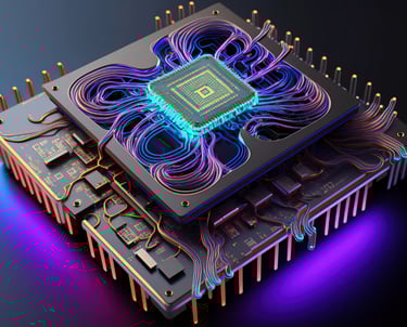
Analog Design
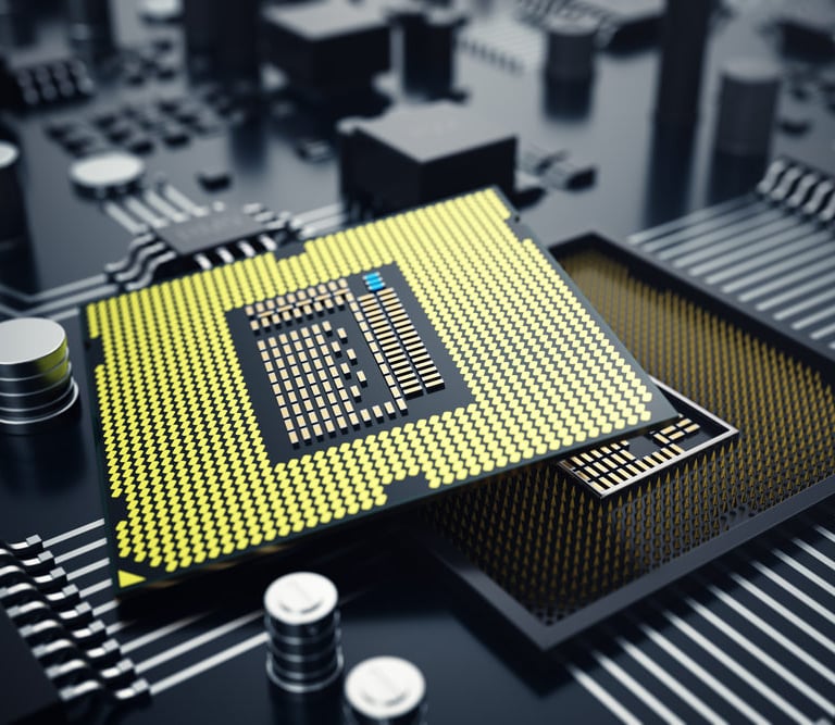
At Karasha, our Analog Layout team is committed to delivering high-precision, silicon-proven layouts that meet stringent performance and reliability standards.
We handle a wide range of analog IP blocks including op-amps, comparators, bandgap references, voltage regulators (LDOs), ADCs/DACs, and PLLs. Our team has hands-on experience with complex layout challenges such as parasitic minimization, high-speed signal routing, and sensitive analog node protection.
We apply best practices in matching, shielding, guard-ring insertion, and floor planning to ensure optimal performance and yield. Working across technology nodes from 300nm down to 5nm, we’ve contributed to multiple successful tape-outs in leading foundries.
Our engineers are well-versed in layout tool suites like Cadence Virtuoso, Calibre, Assura, and PVS, and follow rigorous design methodologies that include LVS, DRC, ERC, and EM/IR checks. We closely collaborate with circuit designers and verification engineers to ensure design intent is preserved and performance goals are achieved. Whether it's standalone IP or part of a larger SoC, our layout solutions are robust, scalable, and ready for mass production.
Precision Layout for High-Performance Analog IPs


At Karasha, our Analog Layout team is committed to delivering high-precision, silicon-proven layouts that meet stringent performance and reliability standards.
We handle a wide range of analog IP blocks including op-amps, comparators, bandgap references, voltage regulators (LDOs), ADCs/DACs, and PLLs. Our team has hands-on experience with complex layout challenges such as parasitic minimization, high-speed signal routing, and sensitive analog node protection.
We apply best practices in matching, shielding, guard-ring insertion, and floor planning to ensure optimal performance and yield. Working across technology nodes from 300nm down to 5nm, we’ve contributed to multiple successful tape-outs in leading foundries.
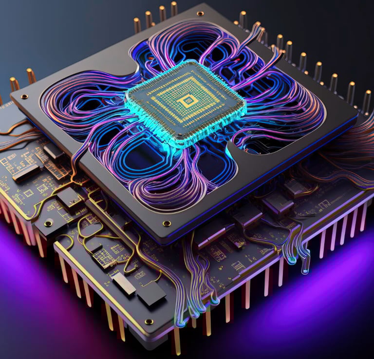
Custom Layout Solutions from 300nm to 5nm
Custom Layout Design
With a proven track record of successful engagements across Tier-1 semiconductor clients, our design verification team offers industry-leading expertise to ensure first-silicon success. We specialize in verifying complex SoCs, ASICs, and IP blocks using advanced methodologies and cutting-edge tools.
Our engineers are proficient with simulators, formal verifiers, debugging platforms, and hardware accelerators from all major EDA vendors, including Synopsys, Cadence, and Siemens EDA. We adopt modern verification methodologies such as UVM, SystemVerilog, and assertion-based verification to ensure comprehensive coverage and accelerated convergence.
Whether you need full turnkey verification, testbench development, or assistance with coverage closure, our team ensures robust, scalable, and reusable environments that align with your schedule and quality goals.
Key Capabilities:
UVM-based Testbench Architecture & Implementation
Formal Verification & Assertion-Based Checking
Coverage-Driven Verification (Functional, Code, Assertion)
Gate-Level Simulation & Low-Power Verification
Debug using waveform viewers and tool-specific platforms
Integration with emulators and FPGA prototyping platforms
Continuous Integration (CI) and Regression Automation
Design Right. Verify Deep. Deliver Fast
Design Verification
At Karasha Tech Solutions, we provide comprehensive Physical Design and Design Verification services tailored to meet the high-performance, low-power, and fast time-to-market demands of today’s semiconductor industry. Our Physical Design team takes full responsibility for the entire backend flow—from RTL/netlist to GDSII—executing industry-proven methodologies for floorplanning, power planning, placement, CTS, routing, and signoff. We are well-versed in handling complex designs across multiple technology nodes, including advanced FinFET processes, with experience in leading foundries like TSMC, Samsung, and GlobalFoundries.
Complementing this, our Design Verification team is known for its delivery excellence across ASIC and SoC projects for Tier-1 clients. With expertise in UVM-based environments, formal verification, simulation acceleration, and emulation platforms, we ensure robust functional correctness and optimal test coverage. Our engineers are skilled in tools like VCS, Questa, Verdi, JasperGold, and Palladium, enabling high-efficiency verification cycles.
Together, our PD and DV teams form a strong foundation for delivering silicon-ready solutions with confidence, precision, and speed.
Physical Design


Address
Karasha Tech Solutions Pvt Ltd
#102, Pt - 28, Narayanadri Towers, Ranga Reddy District, Miyapur, Hyderabad, Telangana 500049, INDIA
Contact
+91 8985090153
info@karashatechsolutions.com
Let’s build something great together
Get in touch
© 2025 Karasha Tech Solutions